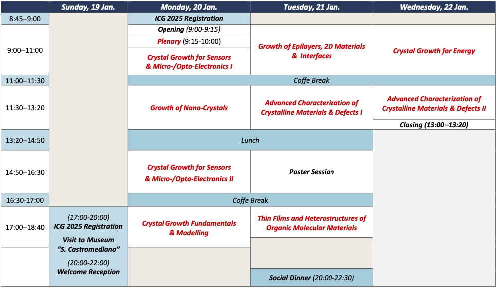
The technical program will include both oral and poster sessions, as well as plenary and invited talks to provide a complete picture of the latest developments in the field.
Invited Plenary Talk
Heike Riel (Science of Quantum and Information Technology Dept., IBM-Zurich, Switzerland)
Invited Keynote Talk
Judy Z. Wu (University of Kansas, Lawrence, USA)
The ICG2025 Program is organized around 7 Scientific Sessions, each one focused on a specific area/application of the growth and/or characterization of crystalline materials. The title and rational of each Session are reported here below:
Session on Crystal Growth Fundamentals and Modelling (Chair: Linda Pastero)
This session will focus on the fundamentals of nucleation and crystal growth from the experimental, theoretical, and computational point of view, from the laboratory to the modelling. We will welcome contributions covering a wide range of topics, included, but not limited to, the following: nucleation and growth of crystals from various media (solution, gel, melt or vapor); effect of mass and heat transport mechanisms; control on crystal growth size and morphology; effect of chemical and physical variables (impurities, temperature, pressure, etc.) on nucleation, growth and crystal quality, defectivity and growth instabilities.
Invited Talk - Romain Grossier (CINAM-CNRS, Marseille, France)
Crystal Growth for Sensors and Micro-/Optoelectronics (Chair: Roberto Fornari)
This Session will cover the latest advancements in the growth of single crystals and thin films of functional materials, with no limitations concerning the employed growth techniques, phase transition and type of precursors. Contributions are expected from the following areas: crystalline semiconductors and oxides for applications as sensors (of pressure, gas, humidity, pH, temperature, acceleration, etc.), electronic devices (including power components for converters and automotive), optoelectronic devices (including light emitters and detectors for the IR-Vis-UV spectrum, and detectors of particles and ionizing radiations).
Invited Talk - Stefano Leone (Fraunhofer-IAF, Freiburg, Germany)
Crystal Growth for Energy (Chairs: Antonio Vecchione and Edmondo Gilioli)
The fast-growing worldwide demand for energy, combined with the limited fossil energy resources, impose the development of efficient devices in the field of renewable energy applications; the progresses in the material synthesis/deposition is essential to enhance their properties. The Session will focus on state-of-the-art studies of materials for the generation and transport of energy, such as crystalline and thin film-based solar cells (inorganic, organic and hybrid), wide gap materials for power electronics applications, superconductors, etc. Besides the bulk crystalline growth and processing and the film deposition by various techniques (vacuum-based, by high energy techniques, from liquid and vapor phase, printing methods, etc.), reports on advanced characterization of materials and devices are also welcome.
Invited Talk - Aldo Di Carlo (CNR-ISM, Rome, Italy)
Growth of Epilayers, 2D Materials and Interfaces (Chair: Giovanni Isella)
The monolithic integration of dissimilar materials on well-established substrates (Si, III-V, SiC, sapphire) lies at the heart of advanced opto-electronic, spintronic, neuromorphic and quantum devices. A deep understanding of the deposition processes and interface formation is essential for the exploitation of physical properties that can enrich conventional technological platforms with novel functionalities. The Session will focus on the heteroepitaxial growth of group IV semiconductors ( Si, Ge, C, Sn, Pb and their alloys), III-V semiconductors (GaN, GaAs, InGaAs, InSb, etc.), oxides, topological materials, 2D materials (graphene, 2D transition metal dichalcogenides, germanene, silicene, stanene, black phosphorous) epitaxially grown or transferred on bulk substrates. Focus will be given to the role played by interfaces in multilayers and 2D/3D heterostructures.
Invited Talk - Jean-Baptiste Rodriguez (University of Montpellier, France)
Growth of Nano Crystals (Chair: Stefano Sanguinetti)
Nanostructures represent a relevant class of materials that provide significant flexibility in the control of their optoelectronic properties by adjusting their composition, size, and dimensionality. They play a key role in advancing cutting-edge technologies across various fields, including lighting and displays, photodetectors, solar cells, telecommunications, (quantum) information processing, (quantum) sensing for fundamental research and versatile applications. This Session focuses on the growth and characterization of nanostructured materials. Topics will include from the synthesis and epitaxial growth of inorganic nanomaterials of different dimensionality (quantum dots, quantum rods, nanowires, nano-platelets/-sheets and quantum wells, and their hybrids) to their applications.
Invited Talk - Artur Tuktamyshev (University of Milano Bicocca, Italy)
Thin films and heterostructures of organic molecular materials (Chair: Adele Sassella)
In the last decades, the successful integration of organic molecular thin films as active layers in various organic devices, from light emitting diodes to transistors to solar cells, has demonstrated the great potentiality of organic molecular materials. The successful study of thin films and devices relies on the availability of controlled growth techniques, which permit to address also the intrinsic material properties. This Session is devoted to the growth of organic molecular thin films and heterostructures, including the growth process itself, but also post growth phenomena, interface effects, and all the physical properties and processes typical of organic molecular materials.
Invited Talk - Alessandro Minotto (University of Milano-Bicocca, Italy)
Advanced Characterization of Crystalline Materials and Defects (Chair: Leander Tapfer)
This Session will discuss topics related to the study of synthetic crystals (inorganic, organic or hybrid) of any size, ranging from bulk to the nanometer scale, and of crystalline interfaces and surfaces. Special emphasis will be given to state-of-the-art characterization methodologies and technologies used to analyze and understand defects and imperfections in crystalline materials generated during growth (or assembling), or induced after material processing. Advanced diagnostic tools and characterizations play a crucial role in uncovering the impact of the structural and morphological properties, and of defects and impurities on the materials’ functional properties and performance.
Invited Talk - Lutz Kirste (Fraunhofer-IAF, Freiburg, Germany)
Invited Talk - Stephen Church (University of Manchester, UK)
